
TSMC’s 1.6nm A16 to change AI chip race
TSMC's A16 process uses backside power delivery to boost speed and cut energy use
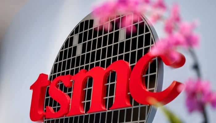
TSMC has completed development and verification of its angstrom-class A16 process, a 1.6nm-class node that could enter mass production within months.
A report from Liberty Times, cited by Chosun, says the chipmaker is targeting the fourth quarter of 2026 to begin volume manufacturing, a timeline that matches TSMC's own public guidance placing A16 production in the second half of the year.
The key innovation behind A16 is Super Power Rail, TSMC's implementation of backside power delivery. Traditional chip designs place both signal and power wiring on the front of the wafer, creating congestion that slows data transmission.
A16 moves the power delivery network to the back of the wafer instead, freeing up front-side space purely for signal routing.
Compared to TSMC's enhanced 2nm process, N2P, the company says A16 delivers an 8% to 10% increase in computing speed at the same voltage, or a 15% to 20% reduction in power consumption at the same speed, along with roughly 8% to 10% higher chip density.
A16 combines this backside power architecture with nanosheet gate-all-around transistors similar to those used in TSMC's N2 family.
The company has positioned the node specifically for high-performance computing and AI accelerator chips, where dense power delivery and complex signal routing create the biggest bottlenecks.
That means A16 silicon is likely to show up first in data centre processors rather than the smartphone chips arriving this year from Apple, Qualcomm and MediaTek, all of which remain on 2nm-class processes.
Advancement by TSMC widens the gap with Samsung, whose plans for 1.4 nm manufacturing capacity have been moved back to 2029 from 2027 as indicated by remarks at SAFE Forum 2026.
In such a case, Samsung will be one year behind in comparison with TSMC's goal for 1.4nm in 2028. While Intel is already utilising backside power delivery with the use of PowerVia technology in Panther Lake microprocessors, the size and client portfolio of TSMC remain its competitive advantages.
However, IBM's recently developed sub-nanometre design is expected to become available in five years.


-
 OpenAI calls for US to take lead in global efforts to develop technical standards
 -
 Nvidia CEO Jensen Huang says there's '0% chance' AI destroys humanity by 2030
 -
 COP31 wants tech giants to clean up AI's energy use
 -
 Google launches 5 Googlebook laptops starting at $899
 -
 UN experts say AI safety is ‘unravelling’
 -
 AI ‘feels pain’? Researchers warn of a dangerous possibility
 -
 Amazon blocks Meta's Muse AI agent from checkouts
 -
 Grandparents are turning kids' photos into AI art